Low level firmware debugging (via SWD)


#1

ok, this is not a support topic really just some ramblings on what I doing to try to do firmware debugging (just started) as it might help someone, and also as a reminder to me :smile: and thanks to @johannes for helping me get this going!

(Work in progress, I'll add more, as I learn more )

(no blame taken if you get it wrong and blow up your board... (very unlikely but still!))

Hardware connections

First, locate the 7-pin header labeled X3, close to LEDs. The SWD connector is labeled JP1, near X3, and has 5 pins, and comes without pinheader soldered in.

the board looks something like this, well as closely as ASCII graphics can do.
e.g.

β€”β€”β€”β€”β€”β€”β€”β€”β€”β€”β€”
LEDR LEDG

o o o o o o o (X3)

    JP1
     o (5) NRST
     o (4) SWDIO
     o (3) GND
     o (2) SWCLK
     o (1) VCC
β€”β€”β€”β€”β€”β€”β€”β€”β€”β€”

you will need to solder in standard header pins, then you can connect with female/female jumper cables.

SWD to STLink/v2 connections

SWD - STLINK/V2
5 - 15 (NRST)
4 - 7 (SWDIO)
3 - 8 (GND)
2 - 9 (SWCLK)
1 - 1 (VCC)

openocd for debugging

command line:

/usr/local/opt/open-ocd/share/openocd/scripts/board/stm32f4discovery.cfg

openocd -f ~/stm32f4discovery.cfg

if this works you will see the following, and the COM light will flash RED/GREEN

Open On-Chip Debugger 0.9.0 (2015-08-08-00:27)
Licensed under GNU GPL v2
For bug reports, read
	http://openocd.org/doc/doxygen/bugs.html
Info : The selected transport took over low-level target control. The results might differ compared to plain JTAG/SWD
adapter speed: 2000 kHz
adapter_nsrst_delay: 100
none separate
srst_only separate srst_nogate srst_open_drain connect_deassert_srst
Info : Unable to match requested speed 2000 kHz, using 1800 kHz
Info : clock speed 1800 kHz
Info : STLINK v2 JTAG v23 API v2 SWIM v4 VID 0x0483 PID 0x3748
Info : using stlink api v2
Info : Target voltage: 3.219895
Info : stm32f4x.cpu: hardware has 6 breakpoints, 4 watchpoints

if you get something about low voltage, checkout VCC
example:

Info : Target voltage: 1.009287
Error: target voltage may be too low for reliable debugging

if it doesn’t communication, check SWDIO/SWCLK
example:

Error: init mode failed (unable to connect to the target)
in procedure 'init' 
in procedure 'ocd_bouncer'

if you get both, check all your connections :slight_smile:


How to code Axoloti objects
Official Pin Outs revised (work in progress)
Debugging axo's
How do I make my own GUI controls for the patcher?, or modify/extend existing ones
#2

Hi @technobear

thank you for this...This is the kind of direction I want to take for AXO so it is comforting that somebody else is thinking in the same direction.

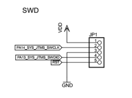
However, I am a bit confused by your indications: according to the schematics, the X3 header has SPI connections (and it is populated on the board), whereas the SWD functionality is on JP1.

Is it just that the post is old and refers to a previous board version?

Thanks,
Mike


#3

Cleared up confusion in top post...


#4

@johannes thank you,

however I am not sure still...In the schematic we have:

So it looks to me that the RST pin is on (5), not (1) as reported above:

JP1
o (1) NRST
o (2) SWDIO
o (3) GND
o (4) SWCLK
o (5) VCC

Also, the connector on ST-Link/v2 and your board schematics report RST, not NRST. Why is it indicated as NRST in the post?

Am I missing something?

Thanks,
Mike


#5

I was confused as you were... in fact i found correct pinouts (as detailed in top post) partly by trial and error :wink:
so this is exactly how ive wired up my axoloti and st-link/v2

(cant comment, on the schematics as i didn't check them, just wanted it working... I'm more a software guy, than hardware :slight_smile: )


#6

Hmm that's bizarre!

I would like @johannes to comment on that, but otherwise will keep flexible when preparing the connection :smiley:

Thank you very much for debugging this!

So...btw...you are treating AXO as if it were an stm32f4discovery board?

Cheers!

M


#7

Updated the pin numbering to correspond with the schematics in the top post.
RST versus NRST, in the schematics there is a (overstrike?) line above RST, this line indicates negative logic.
Or sometimes, where overstrike can't be formatted (like here), it is indicated by a N prefix.
In any case, it is the processor reset signal, in "active-low logic". Active-low for the reset means, reset is active at the low voltage level, so the processor inactive at logic low.
And don't worry, there is no other reset signal involved in SWD setup. And yes, the F4discovery config profile works fine for debugging Axoloti Core.


#8

Cheers @johannes :smiley:

Yes I'm aware of the overbar convention, however my print didn't resolve that very well and it escaped me.
So you've updated the schematics then?

I'll keep going then :wink:

Thank you for your very prompt and courteous replies guys!

M


#9

The overbar probably disappeared when rasterizing to a bitmap picture.


#10

Hi guys,

I have installed the openOCD software, put my hands on an ST-Link/v2, and made the connections as instructed in the top post.

I connect the AXO board with the microUSB, the ST-link through its USB cable (drivers also installed), then head over to a project directory and type:

C:\Projects\E407Blinker\STM32-E407_blink_FLASH>openocd -f stm32f4discovery.cfg
Open On-Chip Debugger 0.9.0 (2015-05-19-12:06)
Licensed under GNU GPL v2
For bug reports, read
        http://openocd.org/doc/doxygen/bugs.html
Info : The selected transport took over low-level target control. The results mi
ght differ compared to plain JTAG/SWD
adapter speed: 2000 kHz
adapter_nsrst_delay: 100
none separate
srst_only separate srst_nogate srst_open_drain connect_deassert_srst
Info : Unable to match requested speed 2000 kHz, using 1800 kHz
Info : clock speed 1800 kHz
Info : STLINK v2 JTAG v25 API v2 SWIM v4 VID 0x0483 PID 0x3748
Info : using stlink api v2
Info : Target voltage: 3.215779
Error: init mode failed (unable to connect to the target)
in procedure 'init'
in procedure 'ocd_bouncer'

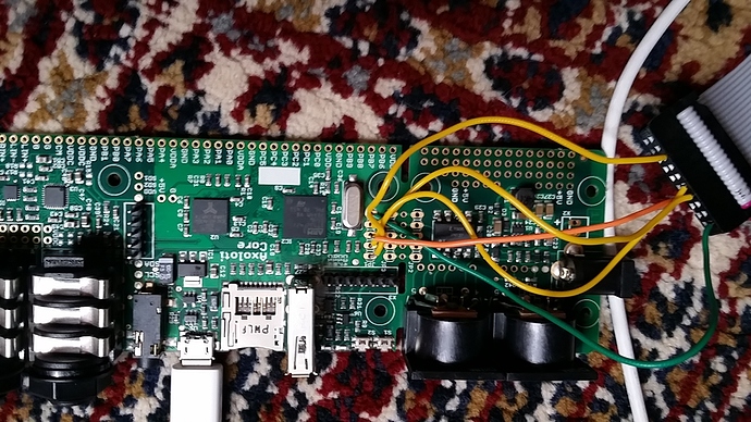
So as @thetechnobear was pointing out, it might well be that my signal connections are crappy. Indeed, they are:

As you see, no soldering...So it is highly likely that this is the issue, however since I do see a supply voltage there, I am just wondering whether there is some other thing I should keep into account...

Any hints?

Thanks,
Mike


#11

Nevermind!!

I got the ST-link cable pinout "upside-down" (exchanged pin rows)