Trying to make CV-in / CV-out addon for Axo


#1

Hi I'm trying to make a design for a CV-in / CV-out addon board for axo (for easy prototyping of AxoBased modules). I had a breadboard design based on the schematics found elsewhere on the forum. I changed the opamp to a TL074 (pdf) because thatis what I had in my workshop.

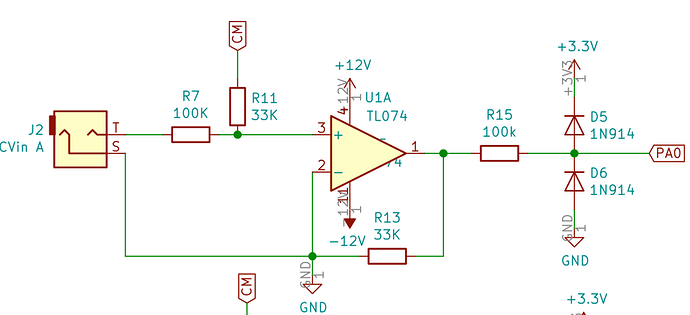
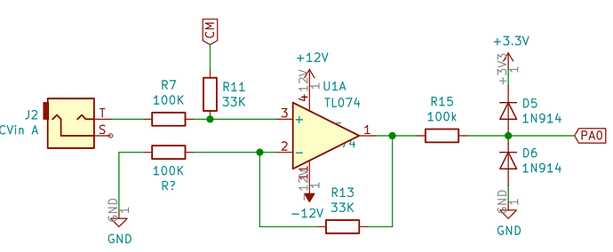
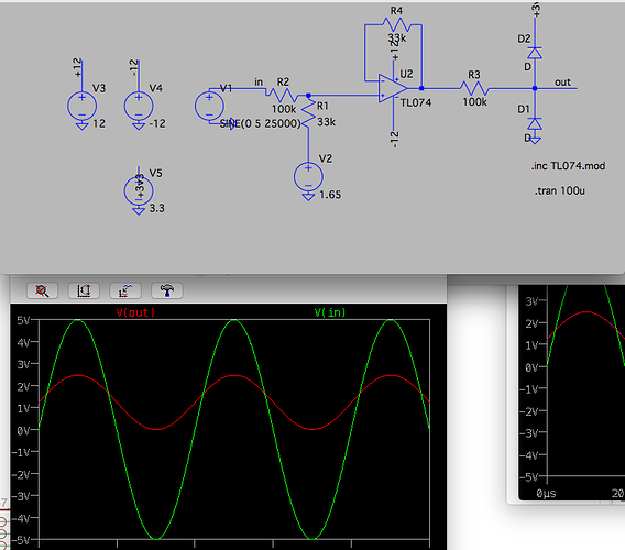
so for CV in I have this:

I tested this on a breadboard and used an arduino to test this (so I would not fry my axo) and this all worked. So transfered it to a protoshield. But it sdoes not work. Now instead of scaling it down, the amp is scaling up, and forgetting all about the 1.65V offset. My signal is almost centered going from -11V to +10V. I have clipping diodes so the axo pin does not get this (-0.6V to 3.3V) but I don't know what is wrong.

Why does an opamp suddenly scale up?

some more info.

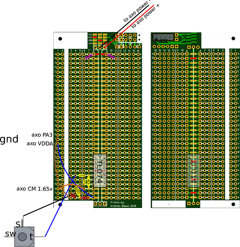
this is my build layout

I'm feeding it a -5v/+5v triangle wave (measured at b3)

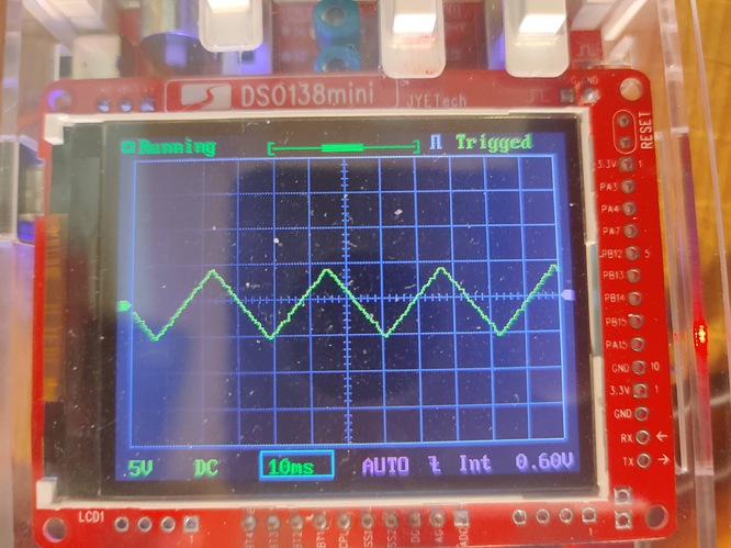
It properly gets scaled and offset before going into the amp (measured at b8 (pin 5 of the TL074)

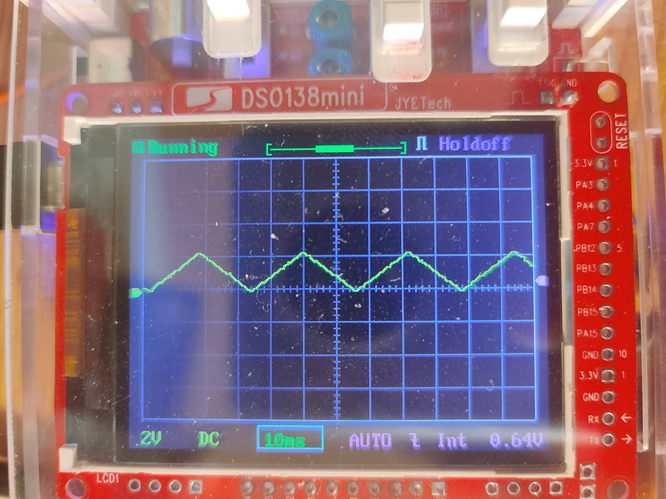
output before the diode clipping is

gnd is measured ok on every gnd point in the schematics
3.3V VDDA is ok
1.65V CM is OK
the resistors are OK
the axo is properly powered from the eurorack, and it works fine, gnd is connected
+12v is measured at a8 on pin 4
-12v is measured at a9 on pin 11

probably something stupid... any ideas?


#2

Your result matches the schematic (I did not figure out the layout yet): with the negative input of the opamp tied to GND, there is no limit to the amplifier's gain, so the output will be extreme (as close to either positive or negative supply as the output stage allows).
I think the dot connecting GND, pin 2 of the TL074, R13 and S of the input socket is wrong. The shield of the input socket should be connected to GND, and the negative input of the opamp should only be connected to R13. That way, the opamp becomes a voltage follower, i.e. output voltage = input voltage.

Edit: the layout looks correct though.


#3

No in the layout I connected the pin to ground on the back. You're right that will be it... Testing later today.


#4

I made a mistake changing the layout from breadboard to schematics...Looking at the original breadboard, I still see one resistor sitting there, so I really forgot to take it out and draw it...
Thanks for spotting the mistake, it works now.

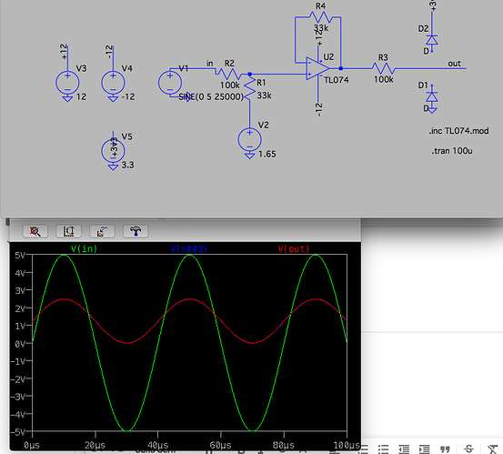
I get a nice linear offset + amplification
but:
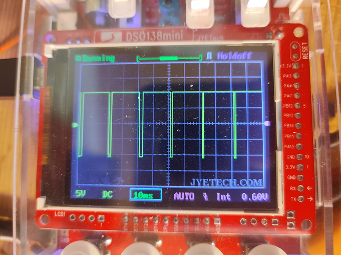
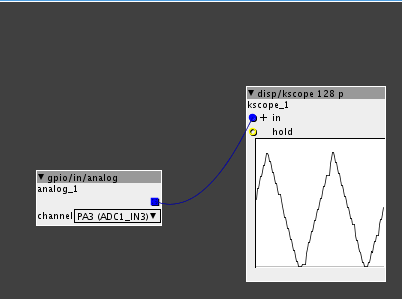
-5v/+5v becomes -0.3v-3v, so not 0-3.3v
as you can see on the axo screenshot, corresponding with my scope output

any idea how I could rectify this? Updated schematics below


#5

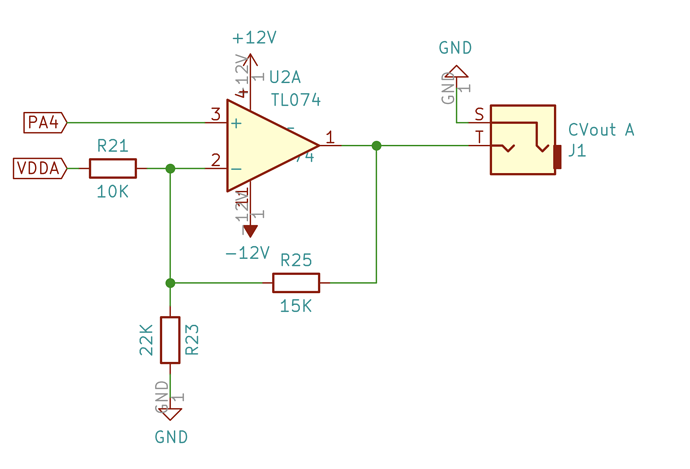
CV Output is working perfectly

meanwhile I have a working 0v/3.3v to -5v/+5v design
this one has no offset problems

I do have a question about the axo safety though. What would happen if I would accidentally plug in a -5/+v signal in the output? Should I add clamping diodes like in the other design? The TL074 is inbetween the pin and the jack, but what could/would happen?

CV-input
CV-input still has the small offset and clipping problem I mentioned earlier

pointers on how to fix are welcome.


#6

I supect the CM voltage: the datasheet of the audio ADC/DAC says to not draw current from the CM output. Maybe 50µA is already too much. Perhaps buffering CM with one of the other opamps of the TL074 will help (the datasheet mentions that connecting the positive input of an opamp is OK, so they probably had this situation in mind).
Or you could do without the CM voltage: one resistor to VDDA and one to GND should achieve the same result, although at the moment I don't remember how to calculate the correct values.


#7

Seems to me, if CM is being used as a 1.65V bias, a voltage divider using 3.3 could easily be tried instead.


#8

Yes that's how it was on the breadboard because I didn't have the reference voltage from an Arduino. Alright so a voltage divider with equal resistors should do the job. Any advice on the values? Like 50 ohm or rather 50Kohm


#9

If you want a replacement for the CM voltage it should be rather low impedance, so it stays at the correct voltage, even if you draw some current from it (like the 50µA that flow through the 33k+100k combination when the Input ist -5V). But a low-impedance voltage divider draws a lot of current, unless it is buffered with an opamp.
Another way would be to not use a 1.65V reference at all. Instead of a 33k resistor (R11) going to CM you would use two resistors of 66k (I've done the math by now), one going to VDDA, the other to GND. Of course, if you build several CV-in channels this would need more resistors (because each channel would need two resistors to reconstruct CM), but it would draw less current than one central voltage divider, because the resistors in each channel draw only as much current as needed.
And 66k is not a standard value, so you'd probably replace R7 by 150k and use 100k towards VDDA and GND or something similar.


#10

What you describe (two resistors of 66k, one going to VDDA, the other to GND), IS a voltage divider; the equal resistors set the voltage at VDDA/2=1.65V. How did you choose 66K? 68K is a close common value.


#11

Yes, the two 66k resistors alone would be a simple voltage divider giving VDDA/2=1.65V. But the resulting voltage is also influenced by CVin via R7 (100k), making this a voltage divider with two inputs, so the math gets a bit complicated (there probably is a simple formula for that case, but I have too little experience with circuit design to know about it).
My quick guess was to consider both resistors as parallel, since they both lead towards a constant voltage (as opposed to the variable input voltage), so they must have twice the original value. This is a somewhat "magical" argument inspired by RF circuit descriptions where all constant voltages are considered GND for RF purposes, since they all are only one capacitor (very low impedance for RF) away from GND.
Of course I didn't trust that kind of magical thinking, so I scribbled the back of an envelope full of equations, put the result into a spreadsheet and checked that it gave the same voltages as a 33k toward a low-impedance CM.


#12

Hi, the problem here is you are using a non inverting configuration that is not well suited to work as a adder/mixer stage (you are trying to add the input voltage plus the reference voltage).
A correct adder/mixer configuration is using an inverting opamp (you have to use 2 in series to get the correct polarity of the signal).

I already did a module with Axoloti that have both CV inputs and CV outputs with correct gain staging and input protection (I used a different protection that yours because using diodes as protection have a few disadvantages).

You can check the circuit here:


#13

Interesting,

What if I would just fix this in the software? Would dropping the second stage suffice?

I see you use -15V/+15V in your modular, would the design change because I'm using -12V/+12V

could you elaborate? Are the diodes contributing to the offset problem? In the simulation, it is not the problem... but it is only a simulation, I don't see the clipping at all in the sim. What other problems could they evoke?


#14

Relevant discussion. See the mentions of virtual ground on the inverting circuit.
https://www.electronics-tutorials.ws/opamp/opamp_4.html


#15

You can't fix the polarity in software because you can get negative voltages into Axoloti. If a negative voltage reaches an input of the GPIO you probably burn it (that is why you should have some input protection).

Diodes have 2 problems:

1 - All diodes have a voltage drop that have to be substracted of the maximum voltage that are connected to (in this case 3.3V). A tipical signal diode have 0.7V of voltage drop, so the maximum voltage that will reach the input of the GPIO will be 2.6V (3.3 - 0.7), so you never going to get the full range of values in Axoloti (It will never reach 127). Even using a schotky diode that have a lower voltage drop (tipical 0.4V) will not be enough to get the full voltage to the input.

2 - When a voltage higher than 3.3V reaches the diodes, the diodes start to conduct and the current will go to the voltage regulator on the Axoloti board, if the current is too high you could burn the regulator and even all chips connected to 3.3V, so you have to limit the current, that is what R15 (100K) is for, but as this resistor have to be a bit high to limit the current enough, it forms a voltage divider with the internal impedance of the GPIO (50K I think), and then again you never reach the full voltage in the input...

In general, using diodes for protection works more or less well when the voltages are higher (5V or more) and when the input impedance of the chip is high...


#16

right, the polarity problem, I should have figured that one out myself.
The diode insights are new to me, good info...

So best way forward seems an inverting opamp for the scale (10V peak to peak that becomes -3.3V to 0V) followed by an inverting unity gain buffer.
I used a lot of words in the previous sentence I haven't used before in my life (at least not in this combination) but I think I understand what I said there :slight_smile: This page explains it very well.

@Sebo Is there any reason you used a TL074 for the first stage and a MCP6002 for the second stage?
I also have some LM13700 lying around, but they are described as Dual Operational Transconductance Amplifier with Linearizing Diodes and Buffers

Even more words I would have to learn about...


#17

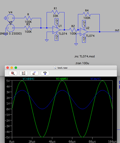
Allright! This one works, modeled according to your schematic, using 2 TL074s

problem here is that it offers no protection , and diodes also don't offer (adequate) protection as discussed earlier.
how could I protect the inputs of the axo.


Gate/Trig Output from Axoloti Pin outputs
#18

The MCP6002 are the "protection". They are opamps that works rail to rail, uses the full range of the power suply they are conected to (the most common opamps like TL074 can't reach the power supply voltages). The power supply for the MCP6002 are +3.3V and ground, so even if they try to put a higher voltage to the output they can't.

The 13700 are transconductance opamps, they are good for make other things like VCAs, VCFs, compressors, etc.