Hi everyone,
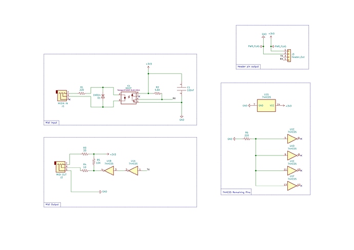
For the last few days, I've been trying to come up with a satisfying circuit diagram for a midi in/out board with 3.5mm trs jack.
As I'm a beginner in electronics, I would like some advice with the circuit diagram I drew. I went through a lot of infos, and tried to pick up as much as I could from the official midi specs and actual 3.3v design implementation, and I'm not sure about some parts of the circuit (mostly in the midi out section).
(the design as been made in kicad so there are kicad specific components like the pwr_flag that aren't physical parts)
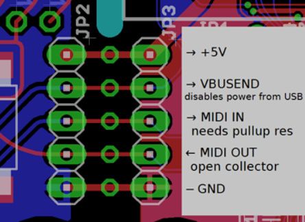
I did this circuit for two reasons. First, to have a midi in/out port after I break the board between jp2 and jp3, and to use in other 3.3v project. (I could also see it being a compatible circuit for the next-gen axo)
My first question is, is there anything that looks horribly wrong ? And if yes, why ?
- In the midi specs it says to use a buffer for the midi out to add additionnal protection, and it also says "It is assumed that the digital buffer driving RC in 3.3V designs is open collector or open drain". Because it is open collector I put a hex inverter gate, but since I use only 2 gates I can use a dual inverter gate (like SN74LVC2G04) ? The reason I used the 74HC05 is because the outputs are open collector and I saw a similar design with a 75HC04 so I tried to stay the closest to it but the unconnected gates might be a waste of space and a source of problem. The hex inverter on this design was used because there was a midi thru port using two more gates.
- The resistor values on the midi output are straight from the official midi specs (except the 10K pullup), but I saw other design with higher values. It's well argumented in the midi specs, but seeing as no other circuit diagram I saw uses those values I am a little bit concerned. Most diagram are using the values for 5V circuits on 3.3V circuits (which apparently is fine, but might not work with every midi device if I understood correctly).

- If I don't use the buffer on the midi output, it simplifies a lot the circuit, but on a diagram for the JP2/JP3 cutting parts, it says midi out / open collector. I'm not sure if it means, that the output is already open collector and therefore needs an open collector output or that it is already open collector.
I must admit I'm confused about the buffer and the open collector part and I'm not 100% sure I fully understand the concept. What I understand is that basically it provides additionnal protection in case something goes wrong (if the midi out cable shorts for example).
If possible I'd like to use a single design for the axoloti and other 3.3V projects.
Any input is welcome and apprectiated.
Thanks if you read all the way through and sorry for the rambling, I'll share the final schematic once it's done, because it's hard to find a diagram with a midi output port.

